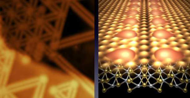
Removing lines of atoms in thin electronic materials creates 'veins' that could benefit solar panels

Could adding defects make a good material even better? Scientists have found that linear defects in a promising thin film create one-atom-thick metallic wires. These wires cross the otherwise intact material, offering a way to channel electrons and photons, tiny packets of light. A multidisciplinary team made this discovery using resources at the Molecular Foundry and the Advanced Light Source.
The team worked with transition metal dichalcogenides (TMDs) because the materials have exceptional optical characteristics. This research found that a single TMD layer could emit as much light as an equivalent material that is 10,000 times thicker, paving the way toward smaller, more efficient devices. Further, the team found that engineering defects (purposely introducing missing or displaced atoms) into TMDs could modify their intrinsic properties. These modifications might improve the material or lead to altogether new useful properties for future energy conversion, quantum computing and communication systems.
In the world of semiconductors, impurities and defects can be a good thing. They modify the properties of materials such as silicon, and scientists can exploit these properties to develop better transistors for laptop computers, smart phones, and solar cells. Recently, scientists discovered a new class of semiconductor that is only three atoms thick and extends in a two-dimensional plane, similar to graphene. These two-dimensional semiconductors, called transition metal dichalcogenides (TMDs), have exceptional optical characteristics. They can be developed into ultra-sensitive photodetectors, and a single TMD layer emits as much light as a three-dimensional TMD crystal composed of 10,000 layers.
For the past several years, scientists have wondered if impurities and defects could also modify TMDs' intrinsic properties, perhaps in ways that improve the semiconductor or lead to new functionalities. Scientists at the Molecular Foundry, in collaboration with researchers at the Advanced Light Source, have taken a big step towards answering this question. They found—to their surprise—how substantial linear defects in TMDs create entirely new properties. Some of these properties indicate that defects in TMDs might even mediate superconducting states.
The team synthesized three-atom-thick, clean layers of molybdenum diselenide, which is a type of TMD. They then studied the material with a microscope that can visualize atoms and their electronic wave functions. They discovered a linear defect formed by a line of missing selenium atoms. This defect creates one-atom-thick metallic wires to transport electrons or photons across the otherwise intact semiconductor like veins.
More information: Sara Barja et al. Charge density wave order in 1D mirror twin boundaries of single-layer MoSe2, Nature Â鶹ŇůÔşics (2016).
Journal information: Nature Â鶹ŇůÔşics
Provided by US Department of Energy


