November 9, 2011 feature
Plasmonic device converts light into electricity

(�鶹��ԺOrg.com) -- While the most common device for converting light into electricity may be photovoltaic (PV) solar cells, a variety of other devices can perform the same light-to-electricity conversion, such as solar-thermal collectors and rectennas. In a new study, engineers have designed a new device that can convert light of infrared (IR) and visible wavelengths into direct current by using surface plasmon excitations in a simple metal-insulator-metal (MIM) device.
The researchers, Fuming Wang and Nicholas A. Melosh of Stanford University, have published their study on the new device in a recent issue of Nano Letters.
“The greatest significance thus far is to show an alternative method to rectennas and PV devices for IR and visible light conversion,” Melosh told �鶹��ԺOrg.com. “The conversion efficiencies aren't amazingly high compared to a PV in visible, so it’s not going to replace PVs, but it could be used for energy scavenging later on.”
The new device’s MIM architecture is similar to that of a rectenna. However, whereas rectennas operate with long-wavelength light such as microwaves and radio waves, the new device operates with a broad spectrum of infrared to visible wavelengths.
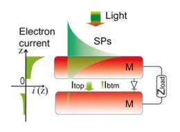
When the MIM device is illuminated, incoming photons are absorbed by the top and bottom metal electrodes. Upon absorption, each photon excites an electron in the metal into a higher energy state so that it becomes a “hot electron.” About half of the hot electrons travel toward the metal-insulator interface, where they may be collected by the other electrode. However, photon absorption in the upper and lower electrodes generates currents with opposite signs, so a net DC current is achieved only if the absorption is larger at one electrode than the other.

This ability to maximize current from one electrode while minimizing it from the other is one of the biggest challenges for MIM devices. To do this, researchers can change the thicknesses of the electrodes. However, there is a tradeoff, since in a thicker electrode, more photons are absorbed but fewer electrons reach the interface due to increased scattering.
Wang and Melosh’s solution is to use a prism to excite surface plamons (SPs) on the metal surface of the electrodes when under illumination. The SPs, which are small electron oscillations, can create a higher concentration of hot electrons in one electrode by efficiently coupling to light. The SP coupling efficiency depends on several factors, such as the thickness of the electrode, the type of metal used, and the wavelength of incoming light.
“SPs are excited by incident light when the photon and SP wave vectors match with each other,” Wang said. “For actual applications, it's more realistic to use nano-grating patterns on one electrode to excite SPs. By simply controlling the pitches of these gratings, SPs can be excited at any specific wavelength. As a result, energy conversion efficiency could be enhanced in the optical band from infrared to visible.”
The engineers calculated that these SP-enhanced MIM devices made with silver electrodes can achieve a power conversion efficiency as high as 4.3% for light with a 640-nm wavelength. Devices with gold electrodes have a maximum efficiency of 3.5% for light with a 780-nm wavelength. Both devices also have good theoretical efficiency across the entire solar spectrum – up to 2.7% for the silver-electrode device. The engineers also calculated that SPs can make silver devices almost 40 times more efficient than without the SPs for infrared light.
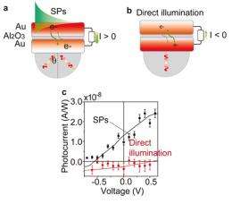
In addition, the researchers fabricated a gold-alumina-gold device, with the top gold layer being slightly thicker than the bottom gold layer. Their experiments confirmed that light hitting the top layer excites SPs on the surface, which cause more hot electrons to be transmitted from the top to the bottom electrode.
Although the resulting photocurrent that the researchers measured was smaller than the theoretical calculated value, they hope to increase the photocurrent in the future by using more effective coupling methods for SPs, optimizing metal thicknesses, and other strategies. Ultimately, the device could prove useful due to the wavelengths at which it operates.
“It can work in the IR better [than other devices that convert light into DC], which can be used for energy scavenging,” Melosh said.
The devices other advantages include easy fabrication and the possibility for being realized on flexible substrates.
From now on, you can too!
More information: Fuming Wang and Nicholas A. Melosh. “Plasmonic Energy Collection through Hot Carrier Extraction.” Nano Letters,
Copyright 2011 �鶹��ԺOrg.com.
All rights reserved. This material may not be published, broadcast, rewritten or redistributed in whole or part without the express written permission of �鶹��ԺOrg.com.


